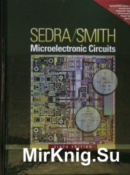
Название: Microelectronic Circuits: 6th Edition
Издательство: Oxford University Press
Автор: Adel S. Sedra and Kenneth C. Smith
Год: 2009
Количество страниц:1456
Язык: English
Формат: pdf
Размер:385 Mb
Ведущий в мире учебник по микроэлектронных схемам продолжает свой уровень знаний и инноваций. Весь материал в 6 - м издании был обновлен , чтобы отразить новейшие технологии. Структура книги была упрощена и сделана более модульной.
The world's leading textbook in microelectronic circuits continues its standard of excellence and innovation. All material in the 6th edition has been updated to reflect the latest technology. The structure of the book has been streamlined and made more modular.
Brief Table of Contents
Part I. Devices and Basic Circuits
1. Signals and Amplifiers
2. Operational Amplifiers
3. Semiconductors
4. Diodes
5. MOS Field-Effect Transistors (MOSFETs)
6. Bipolar Junction Transistors (BJTs)
Part II. Integrated-Circuit Amplifiers
7. Building Blocks of Integrated-Circuit Amplifiers
8. Differential and Multistage Amplifiers
9. Frequency Response
10. Feedback
11. Output Stages and Power Amplifiers
12. Operational Amplifier Circuits
Part III. Digital Integrated Circuits
13. CMOS Digital Logic Circuits
14. Advanced MOS and Bipolar Logic Circuits
15. Memory Circuits
Part IV. Filters and Oscillators
16. Filters and Tuned Amplifiers
17. Signal Generators and Waveform-Shaping Circuits
Full Table of Contents
Part I. Devices and Basic Circuits
Chapter 1. Signals and Amplifiers
Introduction
1.1 Signals
1.2 Frequency Spectrum of Signals
1.3 Analog and Digital Signals
1.4 Amplifiers
1.4.1 Signal Amplification
1.4.2 Amplifier Circuit Symbol
1.4.3 Voltage Gain
1.4.4 Power Gain and Current Gain
1.4.5 Expressing Gain in Decibels
1.4.6 Amplifier Power Supplies
1.4.7 Amplifier Saturation
1.4.8 Symbol Convention
1.5 Circuit Models for Amplifiers
1.5.1 Voltage Amplifiers
1.5.2 Cascaded Amplifiers
1.5.3 Other Amplifier Types
1.5.4 Relationships Between the Four Amplifier Models
1.5.5 Determining Ri and Ro
1.5.6 Unilateral Models 1.6 Frequency Response of Amplifiers
1.6.1 Measuring the Amplifier Frequency Response
1.6.2 Amplifier Bandwidth
1.6.3 Evaluating the Frequency Response of Amplifiers
1.6.4 Single-Time-Constant Networks
1.6.5 Classification of Amplifiers Based on Frequency Response
Summary
Problems
Chapter 2. Operational Amplifiers (Op Amps)
Introduction
2.1 The Ideal Op Amp
2.1.1 The Op-Amp Terminals
2.1.2 Function and Characteristics of the Ideal Op Amp
2.1.3 Differential and Common-Mode Signals
2.2 The Inverting Configuration
2.2.1 The Closed-Loop Gain
2.2.2 Effect of the Finite Open-Loop Gain
2.2.3 Input and Output Resistances
2.2.4 An Important Application: The Weighted Summer
2.3 The Noninverting Configuration
2.3.1 The Closed-Loop Gain
2.3.2 Effect of the Finite Open-Loop Gain
2.3.3 Input and Output Resistances
2.3.4 The Voltage Follower
2.4 Difference Amplifiers
2.4.1 A Single Op-Amp Difference Amplifier
2.4.2 A Superior Circuit: The Instrumentation Amplifier
2.5 Integrators and Differentiators
2.5.1 The Inverting Configuration with General Impedances
2.5.2 The Inverting Integrator
2.5.3 The Op-Amp Differentiator
2.6 DC Imperfections
2.6.1 Offset Voltage
2.6.2 Input Bias and Offset Currents
2.6.3 Effect of Vos and Ios on the Operation of the Inverting Integrator
2.7 Effect of Finite Open-Loop Gain and Bandwidth on Circuit Performance
2.7.1 Frequency Dependence of the Open-Loop Gain
2.7.2 Frequency Response of the Closed-Loop Amplifier
2.8 Large-Signal Operation of Op Amps
2.8.1 Output Voltage Saturation
2.8.2 Output Current Limits
2.8.3 Slew Rate
2.8.4 Full-Power Bandwidth
Summary
Problems
Chapter 3. Semiconductors
3.1 Intrinsic Semiconductors
3.2 Doped Semiconductors
3.3 Current Flow in Semiconductors
3.3.1 Drift Current
3.3.2 Diffusion Current
3.3.3 Relationship Between D and μ
3.4 The pn Junction with Open-Circuit Terminals (Equilibrium)
3.4.1 Physical Structure
3.4.2 Operation with Open-Circuit Terminals
3.5 The pn Junction with Applied Voltage
3.5.1 Qualitative Description of Junction Operation
3.5.2 The Current-Voltage Relationship of the Junction
3.5.3 Reverse Breakdown
3.6 Capacitive Effects in the pn Junction
3.6.1 Depletion or Junction Capacitance
3.6.2 Diffusion Capacitance
Summary
Problems
Chapter 4. Diodes
4.1 The Ideal Diode
4.1.1 Current-Voltage Characteristic
4.1.2 A Simple Application: The Rectifier
4.1.3 Another Application: Diode Logic Gates
4.2 Terminal Characteristics of Junction Diodes
4.2.1 The Forward-Bias Region
4.2.2 The Reverse-Bias Region
4.2.3 The Breakdown Region
4.3 Modelling the Diode Forward Characteristic
4.3.1 The Exponential Model
4.3.2 Graphical Analysis Using the Exponential Model
4.3.3 Iterative Analysis Using the Exponential Model
4.3.4 The Need for Rapid Analysis
4.3.5 The Constant-Voltage Drop Model
4.3.6 The Ideal-Diode Model
4.3.7 The Small-Signal Model
4.3.8 Use of the Diode Forward Drop in Voltage Regulation
4.4 Operation in the Reverse Breakdown Region—Zener Diodes
4.4.1 Specifying and Modeling the Zener Diode
4.4.2 Use of the Zener as a Shunt Regulator
4.4.3 Temperature Effects
4.4.4 A Final Remark
4.5 Rectifier Circuits
4.5.1 The Half-Wave Rectifier
4.5.2 The Full-Wave Rectifier
4.5.3 The Bridge Rectifier
4.5.4 The Rectifier with a Filter Capacitor—The Peak Rectifier
4.5.5 Precision Half-Wave Rectifier—The Super Diode
4.6 Limiting and Clamping Circuits
4.6.1 Limiter Circuits
4.6.2 The Clamped Capacitor or DC Restorer
4.6.3 The Voltage Doubler
4.7 Special Diode Types
4.7.1 The Schottky-Barrier Diode (SBD)
4.7.2 Varactors
4.7.3 Photodiodes
4.7.4 Light-Emitting Diodes (LEDs)
Summary
Problems
Chapter 5. MOS Field-Effect Transistors (MOSFETs)
5.1 Device Structure and Physical Operation
5.1.1 Device Structure
5.1.2 Operation with Zero Gate Voltage
5.1.3 Creating a Channel for Current Flow
5.1.4 Applying a Small ν DS
5.1.5 Operation as ν DS is Increased
5.1.6 Operation for ν DS ≥ V OV
5.1.7 The p-Channel MOSFET
5.1.8 Complementary MOS or CMOS
5.1.9 Operating the MOS Transistor in the Subthreshold Region
5.2 Current-Voltage Characteristics
5.2.1 Circuit Symbol
5.2.2 The iD- ν DS Characteristics
5.2.3 The iD-nuGS Characteristic
5.2.4 Finite Output Resistance in Saturation
5.2.5 Characteristics of the p-Channel MOSFET
5.3 MOSFET Circuits at DC
5.4 Applying the MOSFET in Amplifier Design
5.4.1 Obtaining a Voltage Amplifier
5.4.2 The Voltage Transfer Characteristic (VTC)
5.4.3 Biasing the MOSFET to Obtain Linear Amplification
5.4.4 The Small-Signal Voltage Gain
5.4.5 Determining the VTC by Graphical Analysis
5.4.6 Locating the Bias Point Q
5.5 Small-Signal Operation and Models
5.5.1 The DC Bias Point
5.5.2 The Signal Current in the Drain Terminal
5.5.3 Voltage Gain
5.5.4 Separating the DC Analysis and the Signal Analysis
5.5.5 Small-Signal Equivalent Circuit Models
5.5.6 The Transconductance g m
5.5.7 The T Equivalent Circuit Model
5.5.8 Summary
5.6 Basic MOSFET Amplifier Configurations
5.6.1 The Three Basic Configurations
5.6.2 Characterizing Amplifiers
5.6.3 The Common-Source Configuration
5.6.4 The Common-Source Amplifier with a Source Resistance
5.6.5 The Common-Gate Amplifier
5.6.6 The Common-Drain Amplifier or Source Follower
5.6.7 Summary and Comparisons
5.7 Biasing in MOS Amplifier Circuits
5.7.1 Biasing by Fixing V GS
5.7.2 Biasing by Fixing V G and Connecting a Resistance in the Source
5.7.3 Biasing Using a Drain-to-Gate Feedback Resistance
5.7.4 Biasing Using a Constant-Current Source
5.7.5 A Final Remark
5.8 Discrete-Circuit MOS Amplifiers
5.8.1 The Basic Structure
5.8.2 The Common-Source (CS) Amplifier
5.8.3 The Common-Source Amplifier with a Source Resistance
5.8.4 The Common-Gate Amplifier
5.8.5 The Source Follower
5.8.6 The Amplifier Bandwidth
5.9 The Body Effect and Other Topics
5.9.1 The Role of the Substrate—The Body Effect
5.9.2 Modeling the Body Effect
5.9.3 Temperature Effects
5.9.4 Breakdown and Input Protection
5.9.5 Velocity Saturation
5.9.6 The Depletion-Type MOSFET
Summary
Problems
Chapter 6. Bipolar Junction Transistors (BJTs)
6.1 Device Structure and Physical Operation
6.1.1 Simplified Structure and Modes of Operation
6.1.2 Operation of the npn Transistor in the Active Mode
Current Flow
The Collector Current
The Base Current
The Emitter Current
Recapitulation and Equivalent-Circuit Models
6.1.3 Structure of Actual Transistors
6.1.4 Operation in the Saturation Mode
6.1.5 The pnp Transistor
6.2 Current-Voltage Characteristics
6.2.1 Circuit Symbols and Conventions
The Constant n
Collector-Base Reverse Current (ICBO)
6.2.2 Graphical Representation of Transistor Characteristics
6.2.3 Dependence of i C on the Collector Voltage—The Early Effect
6.2.4 An Alternative Form of the Common-Emitter Characteristics
The Common-Emitter Current Gain β
The Saturation Voltage VCEsat and Saturation Resistance RCEsat
6.3 BJT Circuits at DC
6.4 Applying the BJT in Amplifier Design
6.4.1 Obtaining a Voltage Amplifier
6.4.2 The Voltage Transfer Characteristic (VTC)
6.4.3 Biasing the BJT to Obtain Linear Amplification
6.4.4 The Small-Signal Voltage Gain
6.4.5 Determining the VTC by Graphical Analysis
6.4.6 Locating the Bias Point Q
6.5 Small-Signal Operation and Models
6.5.1 The Collector Current and the Transconductance
6.5.2 The Base Current and the Input Resistance at the Base
6.5.3 The Emitter Current and the Input Resistance at the Emitter
6.5.4 Voltage Gain
6.5.5 Separating the Signal and the DC Quantities
6.5.6 The Hybrid-π Model
6.5.7 The T Model
6.5.8 Small-Signal Models of the pnp Transistor
6.5.9 Application of the Small-Signal Equivalent Circuits
6.5.10 Performing Small-Signal Analysis Directly on the Circuit Diagram
6.5.11 Augmenting the Small-Signal Model to Account for the Early Effect
6.5.12 Summary
6.6 Basic BJT Amplifier Configurations
6.6.1 The Three Basic Configurations
6.6.2 Characterizing Amplifiers
6.6.3 The Common-Emitter Amplifier
Characteristic Parameters of the CE Amplifier
Overall Voltage Gain
Alternative Gain Expressions
Performing the Analysis Directly on the Circuit
6.6.4 The Common-Emitter Amplifier with An Emitter Resistance
6.6.5 The Common-Base (CB) Amplifier
6.6.6 The Common-Collector Amplifier or Emitter Follower
The Need for Voltage Buffers
Characteristic Parameters of the Emitter Follower
Overall Voltage Gain
Thévenin Representation of the Emitter Follower Output
6.6.7 Summary and Comparisons
6.7 Biasing in BJT Amplifier Circuits
6.7.1 The Classical Discrete-Circuit Biasing Arrangement
6.7.2 A Two-Power-Supply Version of the Classical Bias Arrangement
6.7.3 Biasing Using a Collector-to-Base Feedback Resistor
6.7.4 Biasing Using a Constant-Current Source
6.8 Discrete-Circuit BJT Amplifier
6.8.1 The Basic Structure
6.8.2 The Common-Emitter Amplifier
6.8.3 The Common-Emitter Amplifier with an Emitter Resistance
6.8.4 The Common-Base Amplifier
6.8.5 The Emitter Follower
6.8.6 The Amplifier Frequency Response
6.9 Transistor Breakdown and Temperature Effects
6.9.1 Transistor Breakdown
6.9.2 Dependence of β on I C and Temperature
Summary
Problems
Part II. Integrated-Circuit Amplifiers
Chapter 7. Building Blocks of Integrated-Circuit Amplifiers
7.1 IC Design Philosophy
7.2 The Basic Gain Cell
7.2.1 The CS and CE Amplifiers with Current-Source Loads
7.2.2 The Intrinsic Gain
7.2.3 Effect of the Output Resistance of the Current-Source Load
7.2.4 Increasing the Gain of the Basic Cell
7.3 The Cascode Amplifier
7.3.1 Cascoding
7.3.2 The MOS Cascode
7.3.3 Distribution of Voltage Gain in a Cascode Amplifier
7.3.4 The Output Resistance of a Source-Degenerated CS Amplifier
7.3.5 Double Cascoding
7.3.6 The Folded Cascode
7.3.7 The BJT Cascode
7.3.8 The Output Resistance of an Emitter-Degenerated CE Amplifier
7.3.9 BiCMOS Cascodes
7.4 IC Biasing—Current Sources, Current Mirrors, and Current-Steering Circuits
7.4.1 The Basic MOSFET Current Source
7.4.2 MOS Current-Steering Circuits
7.4.3 BJT Circuits
7.5 Current-Mirror Circuits with Improved Performance
7.5.1 Cascode MOS Mirrors
7.5.2 A Bipolar Mirror with Base-Current Compensation
7.5.3 The Wilson Current Mirror
7.5.4 The Wilson MOS Mirror
7.5.5 The Widlar Current Source
7.6 Some Useful Transistor Pairings
7.6.1 The CC-CE, CD-CS, and CD-CE Configurations
7.6.2 The Darlington Configuration
7.6.3 The CC-CB and CD-CG Configurations
Summary
Appendix 7.A: Comparison of the MOSFET and BJT
7.A.1 Typical Values of IC MOSFET Parameters
7.A.2 Typical Values of IC BJT Parameters
7.A.3 Comparison of Important Characteristics
7.A.4 Combining MOS and Bipolar Transistors: BiCMOS Circuits
7.A.5 Validity of the Square-Law MOSFET Model Problems
Chapter 8. Differential and Multistage Amplifiers
8.1 The MOS Differential Pair
8.1.1 Operation with a Common-Mode Input Voltage
8.1.2 Operation with a Differential Input Voltage
8.1.3 Large-Signal Operation
8.2 Small-Signal Operation of the MOS Differential Pair
8.2.1 Differential Gain
8.2.2 The Differential Half-Circuit
8.2.3 The Differential Amplifier with Current-Source Loads
8.2.4 Cascode Differential Amplifier
8.2.5 Common-Mode Gain and Common-Mode Rejection Ratio (CMRR)
8.3 The BJT Differential Pair
8.3.1 Basic Operation
8.3.2 Input Common-Mode Range
8.3.3 Large-Signal Operation
8.3.4 Small-Signal Operation
8.3.5 Common-Mode Gain and CMRR
8.4 Other Nonideal Characteristics of the Differential Amplifier
8.4.1 Input Offset Voltage of the MOS Differential Amplifier
8.4.2 Input Offset Voltage of the Bipolar Differential Amplifier
8.4.3 Input Bias and Offset Currents of the Bipolar Differential Amplifier 8.4.4 A Concluding Remark
8.5 The Differential Amplifier with Active Load
8.5.1 Differential to Single-Ended Conversion
8.5.2 The Active-Loaded MOS Differential Pair
8.5.3 Differential Gain of the Active-Loaded MOS Pair
8.5.4 Common-Mode Gain and CMRR
8.5.5 The Bipolar Differential Pair with Active Load
8.6 Multistage Amplifiers
8.6.1 A Two-Stage CMOS Op Amp
8.6.2 A Bipolar Op Amp
Summary
Problems
Chapter 9. Frequency Response
9.1 Low-Frequency Response of the CS and CE Amplifiers
9.1.1 The CS Amplifier
9.1.2 The CE Amplifier
9.2 Internal Capacitive Effects and the High-Frequency Model of the MOSFET and the BJT
9.2.1 The MOSFET
9.2.2 The BJT
9.3 High-Frequency Response of the CS and CE Amplifiers
9.3.1 The Common-Source Amplifier
9.3.2 The Common-Emitter Amplifier
9.4 Useful Tools for the Analysis of the High-Frequency Response of Amplifiers
9.4.1 The High-Frequency Gain Function
9.4.2 Determining the 3-dB Frequency f H
9.4.3 Using Open-Circuit Time Constants for the Approximate Determination of f H
9.4.4 Miller’s Theorem
9.5 A Closer Look at the High-Frequency Response of the CS and CE Amplifiers
9.5.1 The Equivalent Circuit
9.5.2 Analysis Using Miller's Theorem
9.5.3 Analysis Using Open-Circuit Time Constants
9.5.4 Exact Analysis
9.5.5 Adapting the Formulas for the Case of the CE Amplifier
9.5.6 The Situation when R sig is Low
9.6 High-Frequency Response of the CG and Cascode Amplifiers
9.6.1 High-Frequency Response of the CG Amplifier
9.6.2 High-Frequency Response of the MOS Cascode Amplifier
9.6.3 High-Frequency Response of the Bipolar Cascode Amplifier
9.7 High-Frequency Response of the Source and Emitter Followers
9.7.1 The Source Follower
9.7.2 The Emitter Follower
9.8 High-Frequency Response of Differential Amplifiers
9.8.1 Analysis of the Resistively Loaded MOS Amplifier
9.8.2 Analysis of the Active-Loaded MOS Amplifier
9.9 Other Wideband Amplifier Configurations
9.9.1 Obtaining Wideband Amplification by Source and Emitter Degeneration
9.9.2 The CD-CS, CC-CE and CD-CE Configurations
9.9.3 The CC-CB and CD-CG Configurations
9.10 High-Frequency Response of Multistage Amplifiers
9.10.1 Frequency Response of the Two-Stage CMOS Op Amp
9.10.2 Frequency Response of the Bipolar Op Amp of Section 8.5.2.
Summary
Problems
Chapter 10. Feedback
10.1 The General Feedback Structure
10.2 Some Properties of Negative Feedback
10.2.1 Gain Desensitivity
10.2.2 Bandwidth Extension
10.2.3 Noise Reduction
10.2.4 Reduction in Nonlinear Distortion
10.3 The Four Basic Feedback Topologies
10.3.1 Voltage Amplifiers
10.3.2 Current Amplifiers
10.3.3 Transconductance Amplifiers
10.3.4 Transresistance Amplifiers
10.3.5 A Concluding Remark
10.4 The Feedback Voltage-Amplifier (Series-Shunt)
10.4.1 The Ideal Case
10.4.2 The Practical Case
10.4.3 Summary
10.5 The Feedback Transconductance-Amplifier (Series-Series)
10.5.1 The Ideal Case
10.5.2 The Practical Case
10.5.3 Summary
10.6 The Feedback Transresistance-Amplifier (Shunt-Shunt)
10.6.1 The Ideal Case
10.6.2 The Practical Case
10.6.3 Summary
10.7 The Feedback Current-Amplifier (Shunt-Series)
10.7.1 The Ideal Case
10.7.2 The Practical Case
10.8 Summary of the Feedback Analysis Method
10.9 Determining the Loop Gain
10.9.1 An Alternative Approach for Finding Aβ
10.9.2 Equivalence of Circuits from a Feedback-Loop Point of View
10.10 The Stability Problem
10.10.1 The Transfer Function of the Feedback Amplifier
10.10.2 The Nyquist Plot
10.11 Effect of Feedback on the Amplifier Poles
10.11.1 Stability and Pole Location
10.11.2 Poles of the Feedback Amplifier
10.11.3 Amplifier with a Single-Pole Response
10.11.4 Amplifier with a Two-Pole Response
10.11.5 Amplifier with Three or More Poles
10.12 Stability Study Using Bode Plots
10.12.1 Gain and Phase Margins
10.12.2 Effect of Phase Margin on Closed-Loop Response
10.12.3 An Alternative Approach for Investigating Stability
10.13 Frequency Compensation
10.13.1 Theory
10.13.2 Implementation
10.13.3 Miller Compensation and Pole Splitting
Summary
Problems
Chapter 11. Output Stages and Power Amplifiers
11.1 Classification of Output Stages
11.2 Class A Output Stage
11.2.1 Transfer Characteristic
11.2.2 Signal Waveforms
11.2.3 Power Dissipation
11.2.4 Power Conversion Efficiency
11.3 Class B Output Stage
11.3.1 Circuit Operation
11.3.2 Transfer Characteristic
11.3.3 Power-Conversion Efficiency
11.3.4 Power Dissipation
11.3.5 Reducing Crossover Distortion
11.3.6 Single-Supply Operation
11.4 Class AB Output Stage
11.4.1 Circuit Operation
11.4.2 Output Resistance
11.5 Biasing the Class AB Circuit
11.5.1 Biasing Using Codes
11.5.2 Biasing Using the V BE Multiplier
11.6 CMOS Class AB Output Stages
11.6.1 The Classical Configuration
11.6.2 An Alternative Circuit Utilizing Common-Source Transistors
11.7 Power BJTs
11.7.1 Junction Temperature
11.7.2 Thermal Resistance
11.7.3 Power Dissipation versus Temperature
11.7.4 Transistor Case and Heat Sink
11.7.5 The BJT Safe Operating Area
11.7.6 Parameter Values of Power Transistors
11.8 Variations on the Class AB Configuration
11.8.1 Use of Input Emitter Followers
11.8.2 Use of Compound and Devices
11.8.3 Short-Circuit Protection
11.8.4 Thermal Shutdown
11.9 IC Power Amplifiers
11.9.1 A Fixed-Gain IC Power Amplifier
11.9.2 Power Op Amps
11.9.3 The Bridge Amplifier
11.10 MOS Power Transistors
11.10.1 Structure of the Power MOSFET
11.10.2 Characteristics of Power MOSFETs
11.10.3 Temperature Effects
11.10.4 Comparison with BJTs
11.10.5 A Class AB Output Stage Utilizing Power MOSFETs
Summary
Problems
Chapter 12. Operational Amplifier Circuits
12.1 The Two Stage CMOS Op Amp
12.1.1 The Circuit
12.1.2 Input Common-Mode Range and Output Swing
12.1.3 Voltage Gain
12.1.4 Common-Mode Rejection Ratio (CMRR)
12.1.5 Frequency Response
12.1.6 Slew Rate
12.1.7 Power-Supply Rejection Ratio (PSRR)
12.1.8 Design Tradeoffs
12.2 The Folded Cascode CMOS Op Amp
12.2.1 The Circuit
12.2.2 Input Common-Mode Range and Output Swing
12.2.3 Voltage Gain
12.2.4 Frequency Response
12.2.5 Slew Rate
12.2.6 Increasing the Input Common-Mode Range: Rail-to-Rail Input Operation
12.2.7 Increasing the Output Voltage Range: The Wide-Swing Current Mirror
12.3 The 741 Op-Amp Circuit
12.3.1 Bias Circuit
12.3.2 Short-Circuit Protection Circuitry
12.3.3 The Input Stage
12.3.4 The Second Stage
12.3.5 The Output Stage
12.3.6 Device Parameters
12.4 DC Analysis of the 741
12.4.1 Reference Bias Current
12.4.2 Input-Stage Bias
12.4.3 Input Bias and Offset Currents
12.4.4 Input Offset Voltage
12.4.5 Input Common-Mode Range
12.4.6 Second-Stage Bias
12.4.7 Output-Stage Bias
12.5 Small-Signal Analysis of the 741
12.5.1 The Input Stage
12.5.2 The Second Stage
12.5.3 The Output Stage
12.6 Gain Frequency Response, Slew Rage of the 741
12.6.1 Small-Signal Gain
12.6.2 Frequency Response
12.6.3 A Simplified Model
12.6.4 Slew Rate
12.6.5 Relationship Between f t and SR
12.7 Modern Techniques for the Design of BJT Op Amps
12.7.1 Special Performance Requirements
12.7.2 Bias Design
12.7.3 Design of Input Stage to Obtain Rail-to-Rail ν ICM
12.7.4 Common-Mode Feedback to Control the DC Voltage at the Output of the Input Stage
12.7.5 Output-Stage Design for Near Rail-to-Rail Output Swing
Summary
Problems
Part III. Digital Integrated Circuits
Chapter 13. CMOS Digital Logic Circuits
13.1 Digital Logic Inverters
13.1.1.1 Function of the Inverter
13.1.1.2 The Voltage Transfer Characteristic (VTC)
13.1.1.3 Noise Margins
13.1.1.4 The Ideal VTC
13.1.1.5 Inverter Implementation
13.1.1.6 Power Dissipation
13.1.1.7 Propagation Delay
13.1.1.8 Power-Delay and Energy-Delay Products
13.1.1.9 Silicon Area
13.1.1.10 Digital IC Technologies and Logic-Circuit Families
13.1.1.11 Styles for Digital System Design
13.1.1.12 Design Abstraction and Computer Aids
13.2 The CMOS Inverter
13.2.1 Circuit Operation
13.2.2 The Voltage Transfer Characteristic
13.2.3 The Situation When Q N and Q P are Not Matched
13.3 Dynamic Operation of the CMOS Inverter
13.3.1 Determining the Propagation Delay
13.3.2 Determining the Equivalent Load Capacitance C
13.3.3 Inverter Sizing
13.3.4 Dynamic Power Dissipation
13.4 CMOS Logic-Gate Circuits
13.4.1 Basic Structure
13.4.2 The Two-Input NOR Gate
13.4.3 The Two-Input NAND Gate
13.4.4 A Complex Gate
13.4.5 Obtaining the PUN from the PDN and Vice Versa
13.4.6 The Exclusive-OR Function
13.4.7 Summary of the Synthesis Method
13.4.8 Transistor Sizing
13.4.9 Effects of Fan-In and Fan-Out on Propagation Delay
13.5 Implications of Technology Scaling: Issues in Deep-Submicron Design
13.5.1 Scaling Implications
13.5.2 Velocity Saturation
13.5.3 Subthreshold Conduction
13.5.4 Wiring—The Interconnect
Summary
Problems
Chapter 14. Advanced MOS and Bipolar Logic Circuits
14.1 Pseudo-NMOS Logic Circuits
14.1.1 The Pseudo-NMOS Inverter
14.1.2 Static Characteristics
14.1.3 Derivation of the VTC
14.1.4 Dynamic Operation
14.1.5 Design
14.1.6 Gate Circuits
14.1.7 Concluding Remarks
14.2 Pass-Transistor Logic Circuits
14.2.1 An Essential Design Requirement
14.2.2 Operation with NMOS Transistors as Switches
14.2.3 Restoring the Value of V OH to V DD
14.2.4 The Use of CMOS Transmission Gates as Switches
14.2.5 Pass-Transistor Logic Circuit Examples
14.2.6 A Final Remark
14.3 Dynamic MOS Logic Circuits
14.3.1 The Basic Principle
14.3.2 Nonideal Effects
14.3.3 Domino CMOS Logic
14.3.4 Concluding Remarks
14.4 Emitter-Coupled Logic (ECL)
14.4.1 The Basic Principle
14.4.2 ECL Families
14.4.3 The Basic Gate Circuit
14.4.4 Voltage Transfer Characteristics
14.4.5 Fan-Out
14.4.6 Speed of Operation and Signal Transmission
14.4.7 Power Dissipation
14.4.8 Thermal Effects
14.4.9 The Wired-OR Capability
14.4.10 Final Remarks
14.5 BiCMOS Digital Circuits
14.5.1 The BiCMOS Inverter
14.5.2 Dynamic Operation
14.5.3 BiCMOS Logic Gates
Summary
Problems
Chapter 15. Memory Circuits
15.1 Latches and Flip-Flops
15.1.1 The Latch
15.1.2 The SR Flip-Flop
15.1.3 CMOS Implementation of SR Flip-Flops
15.1.4 A Simpler CMOS Implementation of the Clocked SR Flip-Flop
15.1.5 D Flip-Flop Circuits
15.2 Semiconductor Memories: Types and Architectures
15.2.1 Memory-Chip Organization
15.2.2 Memory-Chip Timing
15.3 Random-Access Memory (RAM) Cells
15.3.1 Static Memory (SRAM) Cell
15.3.2 Dynamic Memory (DRAM) Cell
15.4 Sense Amplifiers and Address Decoders
15.4.1 The Sense Amplifier
15.4.2 The Row-Address Decoder
15.4.3 The Column-Address Decoder
15.4.4 Pulse-Generation Circuits
15.5 Read-Only Memory (ROM)
15.5.1 A MOS ROM
15.5.2 Mask-Programmable ROMs
15.5.3 Programmable ROMs (PROMs and EPROMs)
Summary
Problems
Part IV. Filters and Oscillators
Chapter 16. Filters and Tuned Amplifiers
16.1 Filter Transmission, Types, and Specification
16.1.1 Filter Transmission
16.1.2 Filter Types
16.1.3 Filter Specification
16.2 The Filter Transfer Function
16.3 Butterworth and Chebyshev Filters
16.3.1 The Butterworth Filter
16.3.2 The Chebyshev Filter
16.4 First-Order and Second-Order Filter Functions
16.4.1 First-Order Filters
16.4.2 Second-Order Filter Functions
16.5 The Second-Order LCR Resonator
16.5.1 The Resonator Natural Modes
16.5.2 Realization of Transmission Zeros
16.5.3 Realization of the Low-Pass Function
16.5.4 Realization of the High-Pass Function
16.5.5 Realization of the Bandpass Function
16.5.6 Realization of the Notch Functions
16.5.7 Realization of the All-Pass Function
16.6 Second-Order Active Filters Based on Inductor Replacement
16.6.1 The Antoniou Inductance-Simulation Circuit
16.6.2 The Op Amp-RC Resonator
16.6.3 Realization of the Various Filter Types
16.6.4 The All-Pass Circuit
16.7 Second-Order Active Filters Based on the Two-Integrator-Loop Topology
16.7.1 Derivation of the Two-Integrator-Loop Biquad
16.7.2 Circuit Implementation
16.7.3 An Alternative Two-Integrator-Loop Biquad Circuit
16.7.4 Final Remarks
16.8 Single-Amplifier Biquadratic Active Filters
16.8.1 Synthesis of the Feedback Loop
16.8.2 Injecting the Input Signal
16.8.3 Generation of Equivalent Feedback Loops
16.9 Sensitivity
16.9.1 A Concluding Remark
16.10 Switched-Capacitor Filters
16.10.1 The Basic Principle
16.10.2 Practical Circuits
16.10.3 A Final Remark 16.11 Tuned Amplifiers
16.11.1 The Basic Principle
16.11.2 Inductor Losses
16.11.3 Use of Transformers
16.11.4 Amplifiers with Multiple Tuned Circuits
16.11.5 The Cascode and the CC-CB Cascade
16.11.6 Synchronous Tuning
16.11.7 Stagger-tuning
Summary
Problems
Chapter 17. Signal Generators and Waveform-Shaping Circuits
17.1 Basic Principles of Sinusoidal Oscillators
17.1.1 The Oscillator Feedback Loop
17.1.2 The Oscillation Criterion
17.1.3 Nonlinear Amplitude Control
17.1.4 A Popular Limiter Circuit for Amplitude Control
17.2 Op-Amp–RC Oscillator Circuits
17.2.1 The Wien-Bridge Oscillator
17.2.2 The Phase-Shift Oscillator
17.2.3 The Quadrature Oscillator
17.2.4 The Active-Filter-Tuned Oscillator 17.2.5 A Final Remark
17.3 LC and Crystal Oscillators
17.3.1 LC-Tuned Oscillators
17.3.2 Crystal Oscillators
17.4 Bistable Multivibrators
17.4.1 The Feedback Loop
17.4.2 Transfer Characteristics of the Bistable Circuit
17.4.3 Triggering the Bistable Circuit
17.4.4 The Bistable Circuit as a Memory Element
17.4.5 A Bistable Circuit with Noninverting Transfer Characteristics
17.4.6 Application of the Bistable Circuit as a Comparator
17.4.7 Making the Output Levels More Precise
17.5 Generation of Square and Triangular Waveforms Using Astable Multivibrators
17.5.1 Operation of the Astable Multivibrator
17.5.2 Generation of Triangular Waveforms
17.6 Generation of a Standardized Pulse—The Monostable Multivibrator
17.7 Integrated-Circuit Timers
17.7.1 The 555 Circuit
17.7.2 Implementing a Monostable Multivibrator Using the 555 IC
17.7.3 An Astable Multivibrator Using the 555 IC
17.8 Nonlinear Waveform-Shaping Circuits
17.8.1 The Breakpoint Method
17.8.2 The Nonlinear-Amplification Method
17.9 Precision Rectifier Circuits
17.9.1 Precision Half-Wave Rectifier—The "Superdiode"
17.9.2 An Alternative Circuit
17.9.3 An Application: Measuring AC Voltages
17.9.4 Precision Full-Wave Rectifier
17.9.5 A Precision Bridge Rectifier for Instrumentation Applications
17.9.6 Precision Peak Rectifiers
17.9.7 A Buffered Precision Peak Detector
17.9.8 A Precision Clamping Circuit
Summary
depositfiles.com
turbobit.net
[related-news]
Похожие публикации
- {related-news}
Комментарии 0
Комментариев пока нет. Стань первым!


